As device geometries press against physical limits, material innovation is taking the lead. New compounds and deposition approaches are helping make devices faster, smaller, and more energy-efficient. This article looks at the materials and process choices that are changing thin film workflows and dielectric engineering for high-performance semiconductors.
The Race Beyond Silicon
Scaling silicon alone is getting harder, so engineers are looking to materials that can extend performance without relying only on smaller transistors. High-k dielectrics such as hafnium oxide (HfO₂) and zirconium oxide (ZrO₂) offer lower gate leakage than silicon dioxide (SiO₂), which helps preserve gate control while avoiding ultra-thin oxides that leak current. These layers let designers reduce power draw and fit into multi-gate devices like FinFETs and gate-all-around (GAA) transistors. In one fab scenario, an in-line film uniformity check flagged a recipe drift mid-run, so the process was tuned before downstream tests were affected. For focused process guidance, see this resource.
Advancements in High-k Dielectric Layers
High-k dielectrics improve effective gate capacitance without forcing the physical oxide to be atomically thin, which in turn reduces leakage and helps lower power consumption. That makes them a practical choice for dense transistor architectures. The challenge is controlling the interface and thickness during deposition so you don’t trade leakage for trap states or mobility loss. For example, an on-tool monitor identified a sudden shift in interfacial chemistry and the recipe was adjusted during the same wafer lot to keep electrical targets on track. Explore Precise Thin Film Analysis for concrete metrology and integration approaches.
Innovations in Low-k and Ultra-low-k Dielectrics
Low-k and ultra-low-k dielectrics reduce parasitic capacitance between closely spaced interconnects, which cuts signal delay and lowers crosstalk. Approaches include porous carbon-doped oxides and deliberate air gaps to pull down the effective dielectric constant. Those solutions can be fragile, though, so fabs must balance process steps—like etch, CMP, and thermal budgets—to avoid mechanical or reliability failures. In a typical line example, a post-CMP mechanical check caught weakened film strength, prompting a change to the integration sequence. For more details on integrating these layers, visit more details.
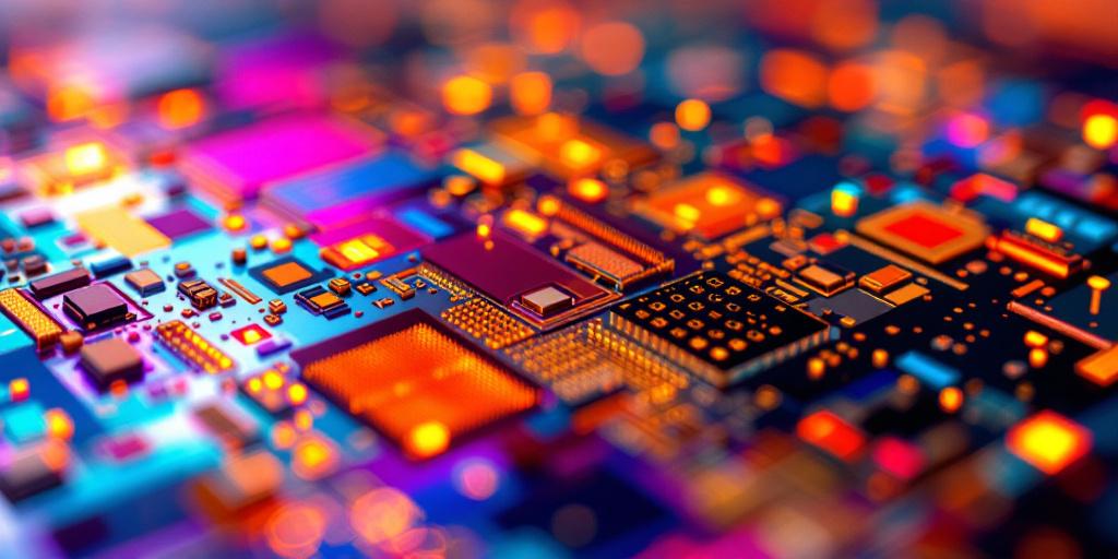
Evolving Approaches to Thin Film Deposition
Thin film deposition is moving toward methods that give tighter control over thickness and composition across complex topographies. Atomic layer deposition (ALD), chemical vapor deposition (CVD), and molecular beam epitaxy (MBE) are common choices. ALD (atomic layer deposition) excels at conformal, uniform films on 3D features. CVD scales well for larger-area coatings, and MBE gives very fine control for engineered heterostructures. Modern in-line metrology and real-time feedback are being used to spot drift in film thickness or composition so recipes can be corrected before yield is affected. A short fab example: a real-time thickness monitor tripped a warning and the chamber sequence was re-run to restore uniformity.
Material Trends in 2D and Quantum Platforms
Two-dimensional materials like MoS₂ and WS₂ and topological insulators bring new electronic behaviors—direct bandgaps in some cases and favorable carrier transport in others—that could change how devices are designed at the micro- and nanoscale. These materials can be grown or transferred as very thin sheets, which reduces material use and opens hybrid integration paths with silicon platforms. Teams are experimenting with hybrid stacks and tailored processes to get practical, reproducible films without disrupting existing process flows. One anonymized example: a transfer step was re-sequenced so a delicate 2D layer avoided a high-temperature anneal that would have degraded performance.
Conclusions
As features push toward atomic dimensions, materials and the processes that put them in place matter more than ever. From high-k dielectrics to 2D semiconductors, the future depends on mastering deposition, metrology, and integration so you can catch drift and fix recipes before they impact test. Staying current with process-focused solutions helps keep new materials on track.