Author
Lex S.
I’m a senior semiconductor R&D specialist with over 25 years in analytical instrumentation and process development. My work involves developing and modifying instruments like SEM, FIB, AFM, and EDX, as well as techniques like reflectometry and Broad Ion Milling.
Optical sensors and imaging systems are evolving fast, becoming essential in fields like semiconductor metrology, security, and industrial automation. New approaches, including distributed fiber optic sensing and Rayleigh-based acoustic detection, are changing how we gather data. Here, we’ll look at how these technologies are pushing the boundaries of precision measurement and optical analysis.
New Horizons in Distributed Optical Sensing
Lately, I’ve seen a lot more interest in Distributed Fiber Optic Sensor (DFOS) systems. Market projections point to significant growth, driven by the oil and gas industry’s need for reliable temperature sensing and new uses for Rayleigh scattering in acoustic detection for railways and security.
At their core, these systems use Rayleigh, Brillouin, and Raman scattering to monitor environmental conditions over long distances. This allows for real-time data on temperature, strain, and vibrations, which is crucial for keeping operations safe and efficient. For example, a pipeline operator can detect a temperature anomaly hundreds of miles away, flagging a potential leak before it becomes a major issue. I see a lot of potential for this in industrial metrology and security, where this level of precise, distributed sensing could make a real difference. As the applications grow, the future for DFOS looks bright. For a detailed market analysis, check out ref. source.
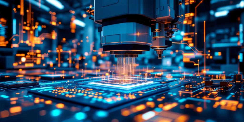
Impact on Semiconductor Metrology and Thin Film Analysis
Advances in optical sensors are having a big impact on semiconductor metrology and thin film analysis. We need more precise optical measurements to characterize materials at the nanoscale, and these new tools deliver. Reflectometry, for instance, is a non-destructive way to measure the layers in a material stack. The application of techniques like WLRS (White-Light Reflectometry System) technology improves the accuracy of this analysis, which is critical in a cleanroom.
In my work, I’ve seen how reflectometry can catch subtle deviations in thin films, helping engineers fine-tune their deposition processes. For example, an in-line system might flag that a film is drifting out of spec, allowing for a recipe correction before the entire wafer run is compromised. Better imaging sensors also mean faster, more accurate inspections on the manufacturing line. By catching errors early and streamlining checks, these technologies help fabs keep up with demand without sacrificing quality. For more information on WLRS technology, check out this link.
Imaging Intelligence in the Era of High-Fidelity Optics
We’re seeing a powerful combination of high-fidelity optical sensors and AI analytics. The growth in hyperspectral, infrared, and 3D imaging is changing how we handle detailed surface and defect inspections. These tools can precisely identify a material’s composition and find tiny structural flaws, which feeds directly into better quality control.
In practice, machine learning algorithms analyze the data from these imaging systems. I’ve seen manufacturing teams use these insights to predict equipment failures before they happen, which cuts down on expensive downtime. Instead of just flagging a bad part, the system can point to a process tool that’s starting to drift. The next step is integrating this with cleanroom automation. Real-time data from optical diagnostics could trigger automated adjustments to a process tool. With edge computing helping to process data locally, this kind of closed-loop control is becoming more practical. As we look ahead, these integrated systems have huge potential to change how we approach industrial diagnostics and operations. For more insights on the technology enabling this revolution, check out more on WLRS technology.
Conclusions
From distributed sensing for infrastructure safety to reflectometry in semiconductor fabs, innovations in optical sensing and imaging are changing how we measure the world. When combined with precision metrology and smart analytics, these tools are driving real progress in science and industry. If you’re looking for precise solutions for your own application, check out our products page or contact us today.