Modern electronics begin with something as simple as sand. Through intricate and highly controlled processes, that sand transforms into sophisticated semiconductor devices that power everything from smartphones to satellites. This article explores how raw silicon becomes a microchip, emphasizing precision, cleanroom environments, and the critical role of optical measurement in quality assurance.
The Birth of Silicon Wafers
Transforming raw silica into ultra-pure silicon is a meticulous and multi-stage process pivotal for semiconductor manufacturing.
Initially, silica, extracted from sand, undergoes a purification process involving high-temperature reduction with carbon. This yields metallurgical-grade silicon, which is then subjected to further refining to achieve semiconductor-grade silicon with over 99.9999% purity.
The next phase involves the Czochralski process, where the purified silicon is melted in a crucible, and a seed crystal is dipped into the molten silicon, slowly pulling it upwards to form a single crystal ingot.
This ingot is then sliced into thin wafers, typically 200mm or 300mm in diameter, with careful attention to achieving uniform thickness. Post-slicing, the wafers undergo a polishing process to ensure mirror-like flatness, crucial for chip functionality.
At this stage, semiconductor metrology becomes indispensable, utilizing techniques to monitor wafer thickness and uniformity. These initial assessments set a foundation for the subsequent fabrication processes, ensuring the highest levels of wafer purity and flatness. The role of thin film analysis begins here, as even minor deviations can impact the performance of the final semiconductor devices.
Building Microstructures with Photolithography and Deposition
Building semiconductor microstructures involves a complex cycle of processes designed to fabricate intricate layers on silicon wafers. Utilizing photolithography, patterns are first transferred onto a light-sensitive photoresist. This step is crucial as the precision in line width directly impacts the performance of transistors and interconnects. Following this, etching processes remove unwanted material, creating the desired microstructures on the wafer.
To build the necessary layers, both Chemical Vapor Deposition (CVD) and Physical Vapor Deposition (PVD) techniques are employed. CVD enables the formation of high-quality thin films essential for electrical isolation and device functionality, while PVD allows for precise metallization. Keeping error margins minimal in etch depth and pattern alignment is vital. This is where semiconductor metrology comes into play. Tools for thin film analysis, such as WLRS technology, utilize reflectometry and optical measurement methods to ensure that each layer meets stringent specifications, optimizing the performance of the chips in the making.
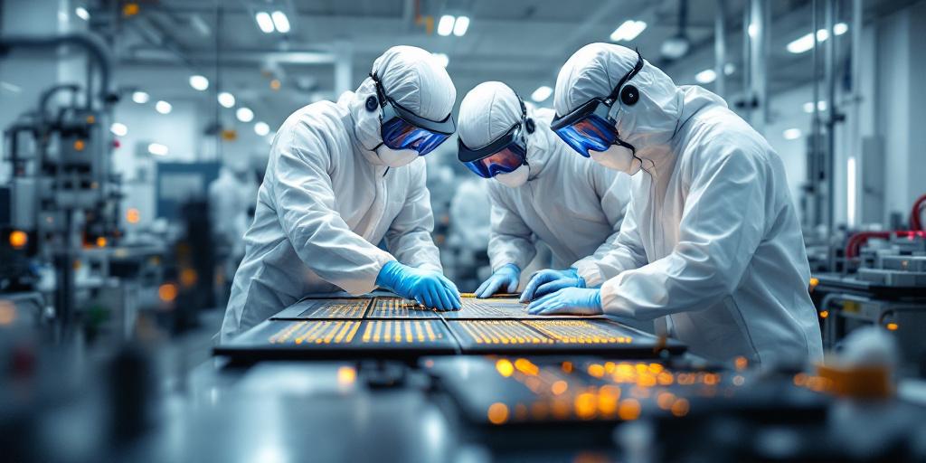
Metrology, Automation, and Quality Assurance in the Cleanroom
In the concluding stages of semiconductor fabrication, metrology plays a pivotal role in ensuring that every wafer meets stringent quality standards. Precision metrology systems are employed to detect defects and variations in nanoscale features, critical for high-performing chips. Advanced metrology techniques, such as reflectometry and optical measurement systems, enable real-time analysis, facilitating high-throughput inspections while maintaining a contamination-free cleanroom environment.
Cleanroom automation synergizes with these optical measurement systems, streamlining workflows and enhancing efficiency. Companies like Reflectonix are at the forefront of this technology, providing solutions for thin film analysis that leverage WLRS technology. This integration not only improves manufacturing accuracy but also ensures that yield analysis is precise, allowing manufacturers to identify and mitigate potential issues before the production scale.
Conclusions
Semiconductor fabrication is a delicate balance of chemistry, physics, and engineering precision that transforms basic materials into cutting-edge technology. From initial wafer creation to intricate patterning and final inspection, each step relies on advanced semiconductor metrology and optical measurement tools. Solutions like WLRS technology and cleanroom automation are vital to meeting today’s demand for performance and reliability in microelectronics. Learn more on our products page or contact us today.